Goldin Here
I spend a lot of time (as many of you do, too) on AI’s power problem — both the enormous electricity demands posed by the technology, as well as the massive inefficiencies of current approaches. In search of what comes next, I’ve gone the distance on orbital solutions, photonics, and even exotic neurology-inspired semiconductor design.
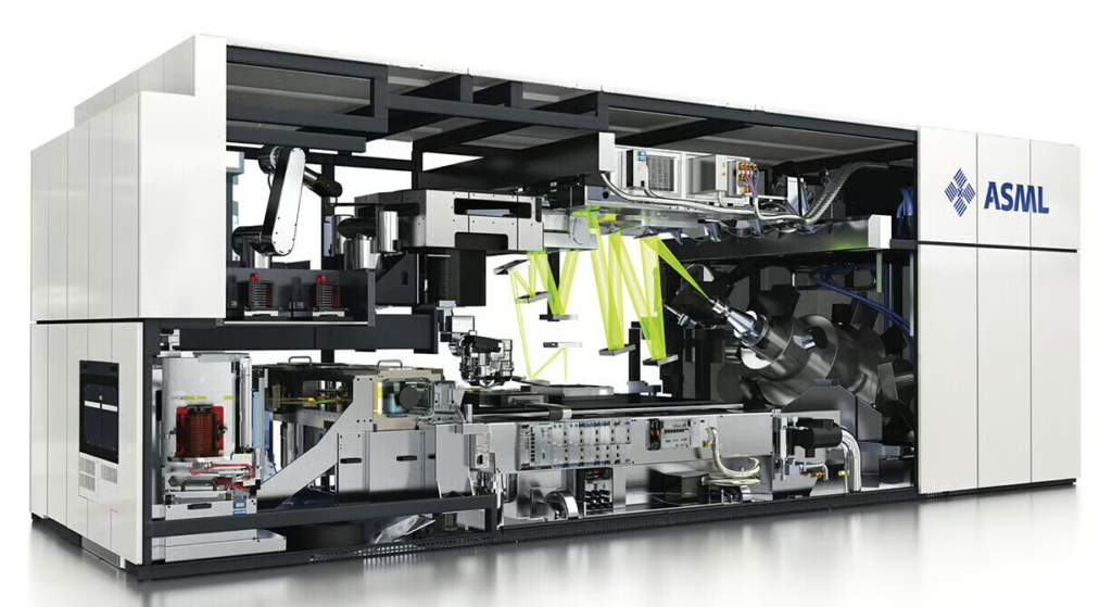
But even if we solved the electron problem, we’d still be bottlenecked by flops (a function of how many chips the industry can actually produce). So I’ve been looking into this side of the equation, which starts in the Dutch town of Veldhoven. There you will find ASML, holder of one of the purest monopolies in industrial history. Every EUV machine on Earth — the machines which prints leading-edge AI chips at scale — comes from ASML’s assembly halls.
Fifty a year
ASML’s Extreme Ultraviolet (EUV) machines are the most precise tools humans have ever built for printing circuits. They draw with 13.5 nm light — a 14× shorter wavelength than the 193 nm Deep Ultraviolet standard before it. Shorter wavelength means finer lines → smaller transistors → denser chips → more AI compute.
High-volume EUV mfg really only began in ’18–’19, laying the groundwork for today’s AI accelerators. Without EUV, we would have no Nvidia H100, no Blackwells, and no AI supercycle.
The thing is, each machine borders on impossible to build:
- The multilayer mirrors that reflect the light (our main protagonist here) are made by a single German firm, Carl Zeiss SMT, and require months of atomic-level polishing and coating — so flat that Mount Everest, shrunk to their scale, would stand one atom tall (anyone who’s done mirror polishing understands the pain 👋)
- It’s a monopoly resting on monopolies: the only EUV-grade optics come from Zeiss in Oberkochen; the only drive lasers from TRUMPF; the light source itself from Cymer of San Diego, which ASML bought outright in 2013 (~$2.5B) to secure it.
- And after all of the high-precision parts arrive from these highly specialized suppliers, final assembly at ASML is no walk in the park — it is a highly sequential process, involving 10,000s of components, tested to nm precision, inside a high-vacuum system in ultra-clean rooms.
Assembly alone takes months, and ASML’s backlog already runs well into ‘27 for TSMC, SK Hynix, Samsung, Intel, and Micron.

ASML shipped 48 of these in 2025. ~50 machines a year is a brutal upstream constraint on new leading-edge AI capacity, worldwide. (With 65 planned for next year and 85 the following. And not one EUV machine has been licensed for export to China.)
But I must ask — does the question necessarily have to be: how many machines can we get out there?
Or is it: how much ultraviolet light for printing geometry on silicon can we generate?
Let There Be (more) Light
Today’s answer to my question — how much light can we generate? — is: barely any.
How it works today: You take droplets of molten tin, each a third the width of a human hair, and fire them across a vacuum chamber 50,000 times a second. A laser strikes each droplet twice, once to flatten it, once to vaporize it into plasma 40× hotter than the surface of the sun. The plasma emits a faint flash of the required 13.5 nm light, and a collector mirror gathers what it can.
All in, less than 1% of the electricity feeding the source comes out as usable EUV.
An extraordinary system of physics, chemistry, and engineering — and a reminder of what babies we still are as creators of compute systems!
Enter the Particle Accelerator
For decades, physics labs have made light with free-electron lasers (FELs), which accelerate electrons to nearly the speed of light and send them weaving through a magnetic array, where they radiate intense, coherent light — tunable to exactly the wavelength you need. Applied to chipmaking, this means far more usable EUV, no tin, no mirror-eating debris, and a source that sits outside the scanners (meaning one FEL can feed several machines at once).
This approach does not attempt to replace the printing machines themselves. Rather, it replaces only their weakest component: the light source, where improvement flows straight into output.
There’s a full-circle quality to this. EUV was born as an American project, with Intel, AMD, Motorola, and the Energy labs (Livermore, Sandia, Berkeley) proving the physics in 1997. Then, a Dutch company spent two decades industrializing the technology. The FEL is American-born, too: invented at Stanford in the ‘70s.
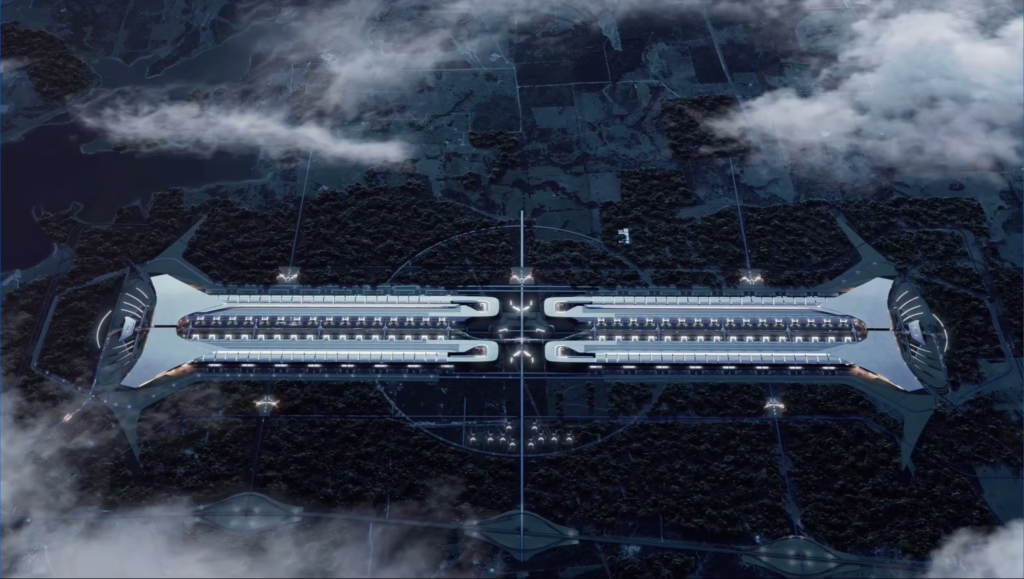
This time around, I have high hopes we can scale FEL at home. I see at least two guys marching in the right direction:
- xLight (backed by Playground Global & Pat Gelsinger) is currently building an FEL prototype, with first light targeted for 2028.
- Elon, meanwhile, appears to be taking the clean-sheet approach. When the above render of Terafab surfaced last week with what looked like a particle accelerator ring beneath the building, (friend of PA) Josh Steinman zeroed in on it and Extropic founder Beff Jezos named the technology — and Musk confirmed… in seven characters: “FEL FTW“
No FEL has yet run a production line, but my belief is when not if, and that the obstacle here is engineering and $$$. Meaningfully more light per machine means meaningfully more chips from our fabs’ existing install base — without needing to build a single new machine.